France: Micromegas Detectors
Micromegas (MICRO MEsh GAseous Structure) detectors were invented in 1995 by Yannis Giomataris at CEA in Saclay, France. It is this type of detector that the group of Alain Debart, based at CEA, are developing for SINE2020 Instrumentation: Detectors. They are continuing work carried out in the previous NMI3 project.
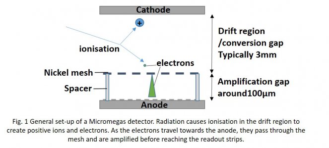
A micromegas detector consists of parallel anode and cathode plates with a metallic nickel micromesh positioned to divide the gas gap between them into two: a drift region where ionization occurs and an amplification region where electrons are amplified on their way to the anode (Figure 1). First constructed designs involved mounting the mesh to insulating quartz spacers attached to the anode; this is the bulk Micromegas. Different voltages applied to the electrodes and mesh create high and low electric field regions to encourage ion and electron movement within the device. As the electric fields are tunable, this allows the performance of the detector to be optimized.

Unfortunately, the mounting of the mesh in this set-up often results in a change of the geometry of the mesh that reduces detector performance. This led to the development of microbulk Micromegas designs that use etching techniques to create an integrated anode-mesh structure – thus avoiding the problem. Bulk and microbulk micromegas designs are used for high-energy physics applications. Bulk has proved to be robust, cheap, easy to operate and suitable for making large area detectors. Microbulk will provide better gap definition and an easier construction process. This is great news for designing new detectors for neutron sources.

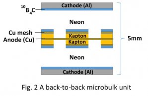
A microbulk Micromegas detector uses a thin flexible polyimide material called Kapton covered on each side with a thin layer of copper metal. This is then fixed to a rigid material that incorporates the anode strips. With the help of a mask to protect some of the material, the unwanted copper and Kapton is removed through lithography and chemical etching techniques to leave a copper micromesh supported by Kapton pillars. The mesh size is about 40 μm. However, to make the detector neutron sensitive, a neutron converter needs to be included (see our article on Resistive Plate Chambers to find out why). SINE2020 researchers at CEA are investigating the deposition of solid 10B4C on to the micromesh and the cathode to double the conversion opportunities. According to simulations, a back-to-back microbulk detector design (Figure 2) with a thickness of 5mm could be 17% efficient.
These microbulk designs do not contain printed circuit boards (PCB) and have very small 50 µm pillars that support the readout components and micromesh, thus reducing “dead space” within the detector. This helps reduce unwanted neutron scattering making it possible to stack several layers to improve the detection efficiency. This is a promising design for development of neutron technologies.
The team at CEA have carried out simulations based on FLUKA MC that predict that four back-to-back units (Figure 3) could achieve 40% efficiency at 1.8Å and, at a 45˚ tilt with respect to the neutron beam, could even reach 45% for 2 µm thick 10B4C layers.

Unfortunately, the scientists encountered problems with B4C peeling off the microbulk material in initial trials. Investigations into understanding why this is occurring are continuing using thicker meshes and different frame materials.
However, a protoype of bulk Micromegas has been built: it consists of a [15 × 15 × 2]cm3 chamber where it is possible for 4 Nickel micromeshes to be stacked. Testing with 2 Nickel micromeshes covered in B4C on both sides (giving a total of 5 layers) in an He-CO2 gas mixture led to a detection efficiency of around 18%.

Using GEM foils
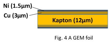
In a related project, the team are also investigating the inclusion of Gas Electron Multipliers (GEM) foils in the design of the detector. A GEM foil consists of insulating Kapton material (12µm thick) clad in copper metal layers (3µm thick) and covered by 1.5µm thick nickel (Figure 4) on both sides in the hope it will improve B4C adhesion. It has conical holes etched into it sized about 40μm and spaced out every 40 μm. When electrons drift into the holes they are amplified efficiently. Simulations indicate that using GEM foils could provide significantly higher electron transmission because of this. Kapton GEM type meshes provide better electron transmission than thin metallic ones. They are also cheap and robust so they could be used for large surfaces (1 × 0.5m2).
Initially, the team verified simulations using a version where only the cathode was boron-coated. The GEM foil was positioned between the electrodes dividing the drift region into two 2mm gaps as shown in Figure 5 below. The experimental results compared well with the simulation results.
A prototype was also created and tested that consists of a double boron-coated nickel mesh and a GEM foil positioned below it to improve the electron transmission as the electrons move to the anode (Figure 6). Results are promising. For both set-ups (Figures 5 and 6) two gas mixtures inside the device were tested: He-CF4 (15%) and Ne-C2H6-CH4 (80/10/10%).

In an ideal set-up the nickel micromesh would be dispensable. In this instance, the GEM foil itself would need to be boron-coated (Figure 7). Unfortunately, the scientists have encountered problems when coating the GEM foils with 10B4C – they have not functioned afterwards. Now the team are exploring coating the GEM foil with just 10B instead.
Future work
As SINE2020 draws to an end, this particular high-efficiency project has stalled. But that does not mean the research has stopped. The team is now working on similar projects exploring simpler designs (e.g. less B4C layers, lower efficiencies) in order to develop high resolution (about 10μm) detectors for neutron imaging and beam profiling.
References:
S Andriamonje et. al.Development and performance of Microbulk Micromegas detectors
Y.Giomataris, Ph.Rebourgeard, J.P.Robert, G.Charpak MICROMEGAS: a high-granularity position-sensitive gaseous detector for high particle-flux environments
G. Tsiledakis, A. Delbart, D. Desforge, I. Giomataris, A. Menelle and T. Papaevangelou A large high-efficiency multi-layered Micromegas thermal neutron detector
Acknowledgements: Alain Menelle, CEA
Back to The Road to the ESS
Other articles: Detectors, CEA/LLB/CNRS


